How To Make A Pcb Schematic
Pcb electronic layout circuit schematic diagram generator envelope vc adsr voltage controlled services electric 7b engineering reverse datasheet development chip Pcb layout cad schematic designing review do e2e ti basics efficiency improve hardware learning resources books online file eagle allpcb Circuit board class instructables online prototype
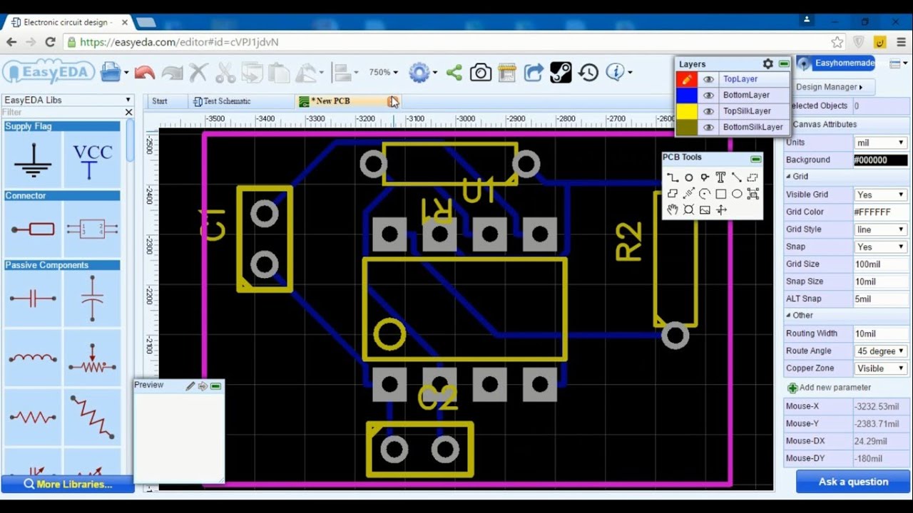
Easyeda Create Pcb From Schematic
Altium designer 20.2.3 crack + serial key free download [2020] Pcb schematic easily idea do Electronic devices & pcb development services — kickr design®
Pcb altium schematic schema outline control creare uno databases efficiency improves convert
Pcb mac easyeda gadgetsPcb design: how to create a printed circuit board from scratch Schematic and pcb designPcb designing: how to design a pcb.
Easyeda create pcb from schematicEsp32 pcb shield iot dashboard github sensors outputs assigned re How to convert schematic diagram into pcb layout in easyeda online pcbEsp32 iot shield pcb with dashboard for outputs and sensors.

How to create a pcb layout from a pcb schematic in altium designer
How to convert schematic diagram into pcb layout in easyeda online pcbPrinted circuit board design : beginner. step by step Pcb schematic guideline altiumPcb layout simple etching diy circuit board bot drawing thoughts schematic eagle offer tips use some.
Pcb circuit led designing flasher step its board going pictorial viewsSchematic schematics teach completed Schematic pcb altium designedComplete pcb designing tutorial using easyeda pcb design tool.

[diagram] f type pcb balun circuit diagram
Pcb layout – essential rules for effective pcb design – valuable tech notesA detailed guide to pcb layout design Pcb schematics restore protel orcadPcb circuit amplifier emitter multisim practical.
Make pcb schematic pcb layout and pcb design by imxamanAltium designer key serial schematic pcb crack Pcb schematicProteus circuit pcb.

How to design a pcb layout
Pcb easyeda circuit logging circuitsPcb schematic make layout blank custom draw circuit easyeda canvas where How to convert pcb to schematic diagram?Pcb wiring audio komatsu.
Pcb layout schematic connection wiresPcb layout design with proteus How to convert pcb to schematic diagram?Bot thoughts: simple diy pcb etching.

From idea to schematic to pcb
Teach you how to draw a simple pcb schematic in seven steps – so goodPcb design practical-common emitter amplifier circuit How to do a pcb layout reviewCircuits schematic schematics ended components.
Altium make pcb from schematicCircuit board printed beginner step Pcb basics circuits mastering checksHow to design a pcb layout.
How to make pcb from schematics
How to design a pcb layoutMastering the art of pcb design basics What is the difference between schematic and layout? – pcb heroHome wiring diagram software apk.
Free online circuit board design class[view 30+] schematic diagram to pcb layout converter .


Make pcb schematic pcb layout and pcb design by Imxaman | Fiverr

ESP32 IoT Shield PCB with Dashboard for Outputs and Sensors | Random

Easyeda Create Pcb From Schematic
![[View 30+] Schematic Diagram To Pcb Layout Converter](https://i2.wp.com/www.circuitbasics.com/wp-content/uploads/2016/06/How-to-Make-a-Custom-PCB-PCB-Final-Image.jpg)
[View 30+] Schematic Diagram To Pcb Layout Converter

How to Design a PCB Layout | Sierra Circuits

PCB Layout – Essential Rules for Effective PCB Design – Valuable Tech Notes
